FPGA Stuff
Learning to make a custom CPU
Building an 8-Bit CPU on an FPGA
I have always wanted to work on FPGA since a long long time, and my semester project for a university level subject called Microprocessors and Computer Architecture, brought along just the perfect opportunity for me to do so.
We had a hardware requirement to have a minimum of 3 sensors in our project. Most people in my class were just doing simple IOT based projects on an Arduino.
But this opportunity was a golden opportunity for me and my friend, we were looking into ways to delve deeper into low level coding since a while and what could be a better opportunity than this.
We got to a work and started planning to make an 8-Bit CPU in RISC-V coded in Verilog using the Vivado Software.
What we used?
- AMD’s Vivado Design Suite 2024 . 2 for Verilog Coding
- FPGA Artix7 Basys 3™ Development Board
What are FPGAs?
A Field-Programmable Gate Array (FPGA) is an integrated circuit that can be programmed and reprogrammed multiple times after manufacturing, typically using hardware description languages like Verilog. What distinguishes FPGAs from Application-Specific Integrated Circuits (ASICs) is their reconfigurable nature.
FPGAs are made up of a grid of Configurable Logic Blocks (CLBs) connected through a flexible, reprogrammable network. This architecture allows for custom routing and logic configurations between the CLBs to meet various application needs.
Or…more specifically the model we working on:
- The Basys3 board is a complete, ready-to-use digital circuit development platform based on the latest Artix-7 Field Programmable Gate Array (FPGA) from Xilinx.
- Can be used to host introductory combinational circuits to complex sequential circuits like embedded processors and controllers.
- Due to the switches, LEDs, and other I/O devices to allow a large number of designs to be completed without the need for any additional hardware.
- The Basys3 also offers an improved collection of ports and peripherals, including: • 16 user switches • 16 user LEDs • 5 user pushbuttons • 4-digit 7-segment display • Three Pmod connectors • Pmod for XADC signals • 12-bit VGA output • USB-UART Bridge • Serial Flash • Digilent USB-JTAG port for FPGA programming and communication • USB HID Host for mice, keyboards and memory sticks
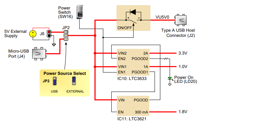
FIg. 1 : Basys3 Power Circuit
Some sample codes
1. Full Adder
Start with creating a new project and initialize the board.
Step1
Start by defining a Design Source fulladder4.v:
`timescale 1ns / 1ps

module full_adder (
    input a,        // First input
    input b,        // Second input
    input cin,      // Carry in
    output sum,     // Sum output
    output cout     // Carry out
);
    assign sum = a ^ b ^ cin;              // XOR for sum
    assign cout = (a & b) | (b & cin) | (a & cin);  // Carry out logic
endmodule

// 4-bit Full Adder Module
module full_adder_4bit (
    input [3:0] a,    // 4-bit first input
    input [3:0] b,    // 4-bit second input
    input cin,        // Initial carry in
    output [3:0] sum, // 4-bit sum output
    output cout      // Final carry out
);
    wire [2:0] carry;  // Internal carry wires between stages

    // Instantiate 4 single-bit full adders
    full_adder fa0 (
        .a(a[0]),
        .b(b[0]),
        .cin(cin),
        .sum(sum[0]),
        .cout(carry[0])
    );

    full_adder fa1 (
        .a(a[1]),
        .b(b[1]),
        .cin(carry[0]),
        .sum(sum[1]),
        .cout(carry[1])
    );

    full_adder fa2 (
        .a(a[2]),
        .b(b[2]),
        .cin(carry[1]),
        .sum(sum[2]),
        .cout(carry[2])
    );

    full_adder fa3 (
        .a(a[3]),
        .b(b[3]),
        .cin(carry[2]),
        .sum(sum[3]),
        .cout(cout)
    );
endmodule
Step 2
Create a testbench file in Simulation Sources `fulladder_tb.v
`timescale 1ns / 1ps

module testbench;
    reg [3:0] a, b;
    reg cin;
    wire [3:0] sum;
    wire cout;

    // Instantiate the 4-bit full adder
    full_adder_4bit fa (
        .a(a),
        .b(b),
        .cin(cin),
        .sum(sum),
        .cout(cout)
    );

    initial begin
        // Test cases
        $monitor("a=%b, b=%b, cin=%b, sum=%b, cout=%b", a, b, cin, sum, cout);

        a = 4'b0000; b = 4'b0000; cin = 0; #10;
        a = 4'b0001; b = 4'b0001; cin = 0; #10;
        a = 4'b0011; b = 4'b0101; cin = 0; #10;
        a = 4'b1111; b = 4'b1111; cin = 0; #10;
        a = 4'b1010; b = 4'b0101; cin = 1; #10;

        $finish;
    end
endmodule
Step 3
Create a constraints file (XDC file) with respective to the Basys 3.
Also we can find the XDC file by searching board name and finding its master.xdc online.
It’s basically us configuring the FPGA buttons and LEDs with respect to our variables like a, b, sum,etc.
# Basys 3 Constraints File for 4-bit Full Adder Demo

# Clock signal (optional, uncomment if using a clocked design)
set_property -dict { PACKAGE_PIN W5    IOSTANDARD LVCMOS33 } [get_ports {clk}]
create_clock -add -name sys_clk_pin -period 10.00 -waveform {0 5} [get_ports clk]

# Switches for inputs
# Input A (a[3:0]) mapped to SW3-SW0
set_property -dict { PACKAGE_PIN V17   IOSTANDARD LVCMOS33 } [get_ports {a[0]}]
set_property -dict { PACKAGE_PIN V16   IOSTANDARD LVCMOS33 } [get_ports {a[1]}]
set_property -dict { PACKAGE_PIN W16   IOSTANDARD LVCMOS33 } [get_ports {a[2]}]
set_property -dict { PACKAGE_PIN W17   IOSTANDARD LVCMOS33 } [get_ports {a[3]}]

# Input B (b[3:0]) mapped to SW7-SW4
set_property -dict { PACKAGE_PIN W15   IOSTANDARD LVCMOS33 } [get_ports {b[0]}]
set_property -dict { PACKAGE_PIN V15   IOSTANDARD LVCMOS33 } [get_ports {b[1]}]
set_property -dict { PACKAGE_PIN W14   IOSTANDARD LVCMOS33 } [get_ports {b[2]}]
set_property -dict { PACKAGE_PIN W13   IOSTANDARD LVCMOS33 } [get_ports {b[3]}]

# Carry-in (cin) mapped to SW8
set_property -dict { PACKAGE_PIN V2    IOSTANDARD LVCMOS33 } [get_ports {cin}]

# LEDs for outputs
# Sum (sum[3:0]) mapped to LD3-LD0
set_property -dict { PACKAGE_PIN U16   IOSTANDARD LVCMOS33 } [get_ports {sum[0]}]
set_property -dict { PACKAGE_PIN E19   IOSTANDARD LVCMOS33 } [get_ports {sum[1]}]
set_property -dict { PACKAGE_PIN U19   IOSTANDARD LVCMOS33 } [get_ports {sum[2]}]
set_property -dict { PACKAGE_PIN V19   IOSTANDARD LVCMOS33 } [get_ports {sum[3]}]

# Carry-out (cout) mapped to LD4
set_property -dict { PACKAGE_PIN W18   IOSTANDARD LVCMOS33 } [get_ports {cout}]

# Set all used pins to use 3.3V logic standard
set_property CFGBVS VCCO [current_design]
set_property CONFIG_VOLTAGE 3.3 [current_design]
Note: You may remove the useless commented stuff for readability and modularity.
Now once the file creations are done respectively, click on:
Run Synthesis, then Run Simulations, we should be able to see the simulation now.
Run Implementations, helps us make sure everything is mapped currently on the FPGA board with respect to our configurations.
Now, to generate a bitstream and program your FPGA board, follow these steps:
Generate the Bitstream: Begin by translating your implemented design into a bitstream that can be downloaded onto your FPGA board.
Open Hardware Manager: Once the bitstream generation is complete, open the Hardware Manager.
Connect Your Board: Ensure your FPGA board is connected to your computer and powered on.
Open Target in Vivado: In Vivado, click on the green callout at the top of the interface, select “Open Target,” and choose “Auto Connect.”
Program the Device: Click “Program Device” in the same callout location. A popup will appear allowing you to load the .bit bitstream file onto the FPGA.
Control the LED: With the bitstream loaded, you can now control the LED on your FPGA board.
2. Simple Adder
simple_adder.v
timescale 1ns / 1ps

module simple_adder (
    input  wire [1:0] a,     // 2-bit input a
    input  wire [1:0] b,     // 2-bit input b
    output wire [2:0] sum    // 3-bit output sum
);
    assign sum = a + b;      // Add inputs a and b
endmodule
testbench.v
`timescale 1ns / 1ps


module testbench;
    reg [1:0] a;        // 2-bit register for input a
    reg [1:0] b;        // 2-bit register for input b
    wire [2:0] sum;     // 3-bit wire for output sum

    // Instantiate the adder
    simple_adder uut (
        .a(a),
        .b(b),
        .sum(sum)
    );

    initial begin
        // Test cases
        a = 2'b00; b = 2'b00; #10; $display("a=%b, b=%b, sum=%b", a, b, sum);
        a = 2'b01; b = 2'b01; #10; $display("a=%b, b=%b, sum=%b", a, b, sum);
        a = 2'b10; b = 2'b01; #10; $display("a=%b, b=%b, sum=%b", a, b, sum);
        a = 2'b11; b = 2'b11; #10; $display("a=%b, b=%b, sum=%b", a, b, sum);
        $finish; // End simulation
    end
endmodule
basys3_constr.xdc
# XDC constraints for Basys 3 Artix-7 FPGA
# This file assumes a 4-bit full adder design with:
# - Inputs: a[3:0], b[3:0], cin
# - Outputs: sum[3:0], cout
# Mapped to switches SW0-SW8 and LEDs LD0-LD4

# Inputs: a[3:0] mapped to SW0-SW3
set_property -dict { PACKAGE_PIN V17 IOSTANDARD LVCMOS33 } [get_ports a[0]]
set_property -dict { PACKAGE_PIN V16 IOSTANDARD LVCMOS33 } [get_ports a[1]]
set_property -dict { PACKAGE_PIN W16 IOSTANDARD LVCMOS33 } [get_ports a[2]]
set_property -dict { PACKAGE_PIN W17 IOSTANDARD LVCMOS33 } [get_ports a[3]]

# Inputs: b[3:0] mapped to SW4-SW7
set_property -dict { PACKAGE_PIN W15 IOSTANDARD LVCMOS33 } [get_ports b[0]]
set_property -dict { PACKAGE_PIN V15 IOSTANDARD LVCMOS33 } [get_ports b[1]]
set_property -dict { PACKAGE_PIN W14 IOSTANDARD LVCMOS33 } [get_ports b[2]]
set_property -dict { PACKAGE_PIN W13 IOSTANDARD LVCMOS33 } [get_ports b[3]]

# Input: cin mapped to SW8
set_property -dict { PACKAGE_PIN V2 IOSTANDARD LVCMOS33 } [get_ports cin]

# Outputs: sum[3:0] mapped to LD0-LD3
set_property -dict { PACKAGE_PIN U16 IOSTANDARD LVCMOS33 } [get_ports sum[0]]
set_property -dict { PACKAGE_PIN E19 IOSTANDARD LVCMOS33 } [get_ports sum[1]]
set_property -dict { PACKAGE_PIN U19 IOSTANDARD LVCMOS33 } [get_ports sum[2]]
set_property -dict { PACKAGE_PIN V19 IOSTANDARD LVCMOS33 } [get_ports sum[3]]

# Output: cout mapped to LD4
set_property -dict { PACKAGE_PIN W18 IOSTANDARD LVCMOS33 } [get_ports cout]

# Clock signal (uncomment if your design uses the 100 MHz clock)
# The Basys 3 has a 100 MHz clock connected to pin W5
# set_property -dict { PACKAGE_PIN W5 IOSTANDARD LVCMOS33 } [get_ports clk]
# create_clock -period 10.00 -name sys_clk [get_ports clk]

# Configuration settings for Basys 3
set_property CFGBVS VCCO [current_design]
set_property CONFIG_VOLTAGE 3.3 [current_design]
So now the coding part is done, after doing the following:
Run Simulation —> Run Synthesis —> Run Implementation —> Generate Bitstream —> Open Target —> Program Device
AND……yay, looking at the demo, let’s try:
a= 0010 b= 1010
sum=1100
Building CPU
You can almost say, got a bit inspired by the a nice implementation on TinyFPGA BX: https://austinmorlan.com/posts/8bit_breadboard_fpga/
Sooo, you know, with Verilog you’re describing the logical behavior of a circuit and relying on the FPGA tools to synthesize your design into the gates on the FPGA that will do what you want. Similar to how you describe a program in C and trust the compiler to generate assembly for you.
Soo while researching for what I wanted to build, I did came across a curious concept of a SAP computers. SAP as in Simple as Possible (SAP) computers in general were designed to introduce beginners to some of the crucial ideas behind computer operations.
The SAP-1 computer is the first stage in this evolution and contains the basic necessities for a functional computer. Its primary purpose is to develop a basic understanding of how a computer works, interacts with memory and other parts of the system like input and output. The instruction set is very limited and is simple.
For conceptual and diagramatic understanding I referred to Digital Computer Electronics by Albert Paul Malvino and Jerald A Brown
SAP 1
The SAP-1 computer is a bus-organized computer and makes use of Von-Neumann architecture. It makes use of an 8-bit central bus and has ten main components. A pictorial representation of its architecture is shown below. Each of the individual components that make up this computer are described right after.
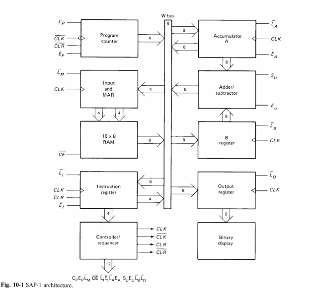
So for this project we tried our luck on implementing SAP-1.
Updating soon!
Source Code: https://github.com/euphoricair7/Processor-Design-on-FPGA